
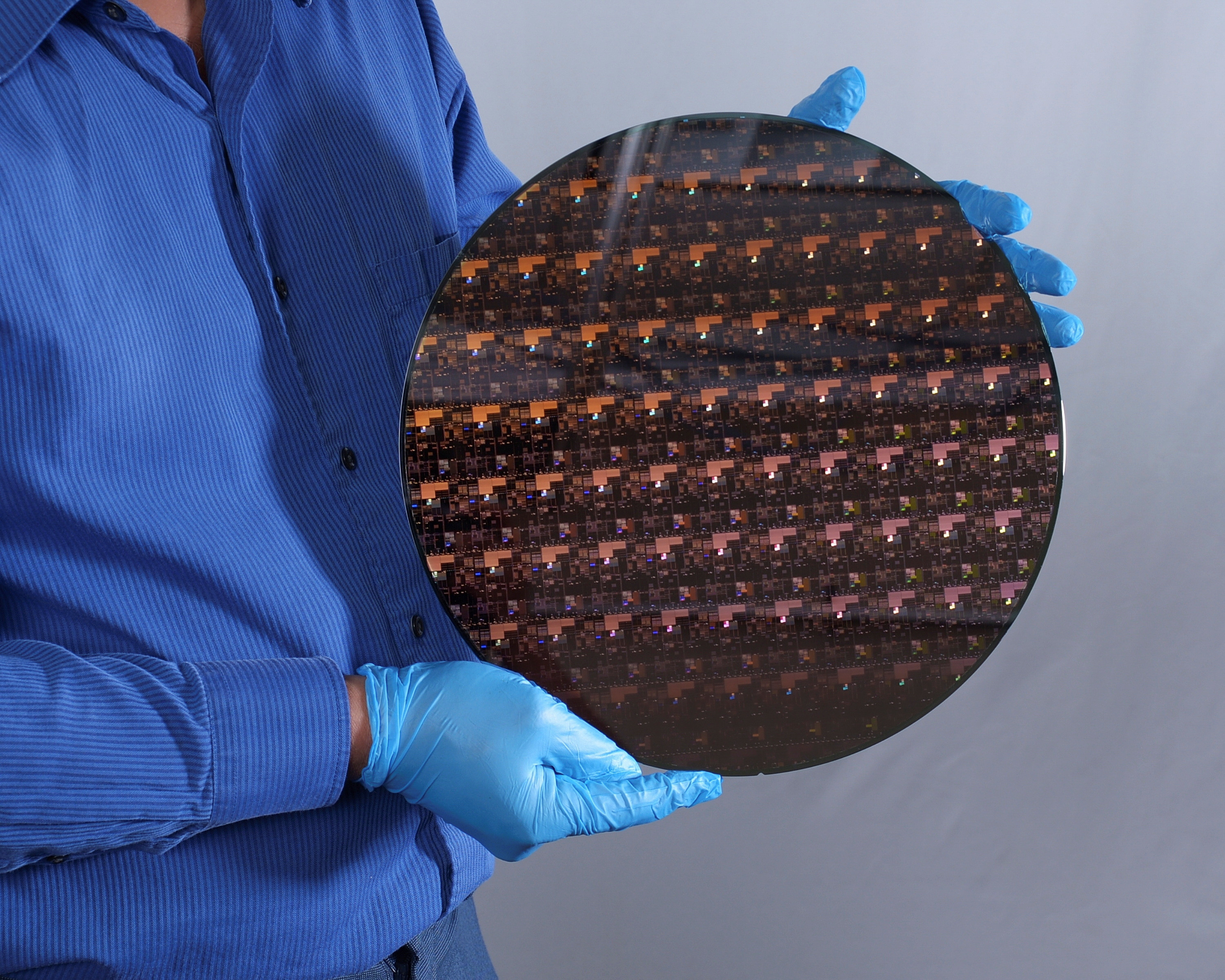
The collaboration leverages IBM’s semiconductor device innovation alongside Siemens’ expertise in lithography optimization and process simulation. The nanostack architecture, unveiled by IBM earlier this year, functions by vertically stacking and staggering transistors. This configuration promises significant gains in both performance and power efficiency compared to traditional layouts.
Scaling this technology from the laboratory to commercial production remains the primary challenge. To bridge this gap, the teams will create advanced virtual models of the nanostack. These digital prototypes allow engineers to simulate performance, refine structural designs, and identify potential fabrication defects before physical manufacturing begins. By addressing these complexities in a virtual environment, the companies hope to streamline the eventual transition to large-scale semiconductor production.
Comments (0)
No comments yet. Be the first!